Tallinn Technical University
high speed photodiode preamp design
Ivan Polevoi
980882 LAS-63
The HP 5082-4204 PIN Photodiode will be used as an example for our discussion. Its characteristics are given in Figure 5.26. It is typical of many commercially available PIN photodiodes. As in most high-speed photodiode applications, the diode is operated in the reverse-biased or photoconductive mode. This greatly lowers the diode junction capacitance, but causes a small amount of dark current to flow even when the diode is not illuminated (we will show a circuit which compensates for the dark current error later in the section).
This photodiode is linear with illumination up to approximately 50 to 100uA of output current. The dynamic range is limited by the total circuit noise and the diode dark current (assuming no dark current compensation).
HP 5082-4204 PHOTODIODE
Sensitivity: 350uA @ 1mW, 900nm
Maximum Linear Output Current: 100uA
Area: 0.002cm2 (0.2mm2)
Capacitance: 4pF @ 10V Reverse Bias
Shunt Resistance: io^11 W
Risetime: 10ns
Dark Current: 6ООрА @ 10V Reverse Bias
Figure 5.26
Using the circuit shown in Figure 5.27, assume that we wish to have a full scale output of 10V for a diode current of 100
m А. This determines the value of the feedback resistor R2 to be 10V/100m А = 100kW .![]() Using the diode capacitance, CD=4pF, and the AD823
input capacitance, CIN =1.8pF, the value of C1 = CD+Cin =
5.8pF. Solving the above equations using C1=5.8pF, R2=100kW , and fu=16MHz, we find that:
Using the diode capacitance, CD=4pF, and the AD823
input capacitance, CIN =1.8pF, the value of C1 = CD+Cin =
5.8pF. Solving the above equations using C1=5.8pF, R2=100kW , and fu=16MHz, we find that:
f1 = 274kHz
C2 = 0.76pF
f2 = 2.1MHz.
In the final design (Figure 5.27), note that the 100kW resistor is replaced with three 33.2kW film resistors to minimize stray capacitance. The feedback capacitor, C2, is a variable 1.5pF ceramic and is adjusted in the final circuit for best bandwidth/pulse response. The overall circuit bandwidth is approximately 2MHz.
The full scale output voltage of the preamp for 100m А diode current is 10V, and the error (RTO) due to the photodiode dark current of 600pA is 60mV. The dark current error can be canceled using a second photodiode of the same type in the non-inverting input of the op amp as shown in Figure 5.27.
2MHz BANDWIDTH PHOTODIODE PREAMP WITH DARK CURRENT COMPENSATION

As in most noise analyses, only the key contributors need be identified. Because the noise sources combine in an RSS manner, any single noise source that is at least three or four times as large as any of the others will dominate.
In the case of the wideband photodiode preamp, the dominant sources of output noise are the input voltage noise of the op amp, VN, and the resistor noise due to R2, VN,R2 (see Figure 5.28). The input current noise of the FET-input op amp is negligible. The shot noise of the photodiode (caused by the reverse bias) is negligible because of the filtering effect of the shunt capacitance C1. The resistor noise is easily calculated by knowing that a 1k
W resistor generates about 4nV/Hz, therefore, a 100kW resistor generates 40nV/Hz. The bandwidth for integration is the signal bandwidth, 2.1MHz, yielding a total output rms noise of:![]() RTO NOISE =
RTO NOISE = ![]() =73m Vrms.
=73m Vrms.
The factor of 1.57 converts the approximate single-pole bandwidth of 2.1MHz into the equivalent noise bandwidth.
The output noise due to the input voltage noise is obtained by multiplying the noise gain by the voltage noise and integrating the entire function over frequency. This would be tedious if done rigorously, but a few reasonable approximations can be made which greatly simplify the math. Obviously, the low frequency 1/f noise can be neglected in the case of the wideband circuit. The primary source of output noise is due to the high-frequency noise-gain peaking which occurs between f i and fu. If we simply assume that the output noise is constant over the entire range of frequencies and use the maximum value for AC noise gain [1+(C1/C2)], then

The total rms noise referred to the output is then the RSS value of the two components:
TOTAL RTO NOISE = ![]()
The total output dynamic range can be calculated by dividing the full scale output signal (10V) by the total output rms noise, 260
m Vrms, and converting to dB, yielding approximately 92dB.EQUIVALENT CIRCUIT FOR OUTPUT NOISE ANALYSIS
C1 = 5.8pF
C2 = 0.76pF
R2 = 100k
W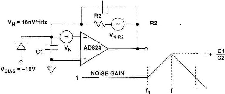
274kHz 2.1MHz 16MHz
VN RTO NOISE = 250
m V RMSVN,R2 RTO NOISE = 74
m V RMSTOTAL RTO NOISE =260
m V RMSDYNAMIC RANGE = 92dB
Figure 5.28
And here some information I found on this site:
http://home.att.net/~ssmodeling/Large value feedback resistor circuits require these types of amplifiers. For biased circuits a bipolar operational amplifier can also be considered especially for Avalanche photodiodes. Bipolar amplifiers are usually only used with feedback resistors of 50k ohms and lower, because the output offsets caused by their high input bias current. Bipolar amplifiers have lower input voltage noise, but higher input current noise FET amplifiers. They are typically much faster than FET and CMOS type amplifiers and maybe considered for high-speed circuitry.
Feedback capacitance values for an overshoot of 5% and 25% are calculated. The 5% overshoot capacitance value is the smallest capacitance recommended in a production circuit. This is because of the tolerance of the components. A capacitance value for a 25% can be used, but the devices will need to be tested for overshoot because the component tolerances may cause the circuit to have excessive ringing and instability. The faster the circuit is the more noise it will have and less stable it will be; therefore don't design the circuit for more bandwidth than is required.
That's basically all you need to know to design transimpedance amplifier circuits. Power supply bypass capacitors recommended by the operational amplifier manufacturer should always be used and are not shown in any of the model or circuitry schematics
|
PHOTOVOLTAIC (no bias) PHOTODIODE/TRANIMPEDANCE AMP MODEL | ||||||
|
Amplifers charteristics |
opa111 |
Units |
Photodiode charteristics |
Units | ||
|
Input noise voltage (Vn) |
6.00E-09 |
V/Hz |
capacitance in Farads (Cp) |
2.50E-11 |
F | |
|
Input current noise (In) |
8.00E-16 |
A/Hz |
shunt resistance in ohms (Rsh) |
1.00E+08 |
| |
|
Gain bandwith product (fu) |
2.00E+06 |
Hz |
responsivity |
5.00E-01 |
A/W | |
|
input bias current (Ib) |
1.00E-12 |
F |
noise equivalent power NEP |
5.00E-15 |
W/Hz | |
|
input offset voltage (Voff) |
2.50E-04 |
A |
rise or fall time Tr |
1.00E-08 |
S | |
|
input capacitance (CA) |
3.00E-12 |
V |
||||
|
Amplifer feedback |
Units | |||||
|
Feedback resistance (Rf) |
1.00E+07 |
| ||||
|
Feedback capacitance (Cf) |
1.00E-12 |
F | ||||

|
OPERATIONAL AMPLIFIER CHARACTERISTICS TABLE |
|||||||||
|
Vn |
|||||||||
|
number of |
input |
at 10 kHz |
In |
fu |
Ib |
Voffset |
CA | ||
|
part number |
Amplifiers |
stage |
manufacturer |
(V/Hz) |
(A/Hz) |
(Hz) |
(A) |
(V) |
(F) |
|
OPA111 |
1 |
FET |
Burr-Brown |
6.00E-09 |
8.00E-16 |
2.00E+06 |
1.00E-12 |
0.00025 |
3.00E-12 |
|
OPA121 |
1 |
FET |
Burr-Brown |
6.00E-09 |
8.00E-16 |
2.00E+06 |
5.00E-12 |
0.00200 |
3.00E-12 |
|
OPA124 |
1 |
FET |
Burr-Brown |
6.00E-09 |
8.00E-16 |
1.50E+06 |
1.00E-12 |
0.00025 |
3.00E-12 |
|
OPA128 |
1 |
FET |
Burr-Brown |
1.50E-08 |
2.20E-16 |
5.00E+05 |
7.50E-14 |
0.00050 |
3.00E-12 |
|
OPA129 |
1 |
FET |
Burr-Brown |
1.50E-08 |
1.00E-16 |
1.00E+06 |
1.00E-13 |
0.00200 |
3.00E-12 |
|
OPA130 |
1 |
FET |
Burr-Brown |
1.60E-08 |
4.00E-15 |
1.00E+06 |
2.00E-11 |
0.00100 |
3.00E-12 |
|
OPA2130 |
2 |
FET |
Burr-Brown |
1.60E-08 |
4.00E-15 |
1.00E+06 |
2.00E-11 |
0.00100 |
3.00E-12 |
|
OPA4130 |
4 |
FET |
Burr-Brown |
1.60E-08 |
4.00E-15 |
1.00E+06 |
2.00E-11 |
0.00100 |
3.00E-12 |
|
OPA132 |
1 |
FET |
Burr-Brown |
8.00E-09 |
3.00E-15 |
8.00E+06 |
5.00E-11 |
0.00050 |
3.00E-12 |
|
OPA2132 |
2 |
FET |
Burr-Brown |
8.00E-09 |
3.00E-15 |
8.00E+06 |
5.00E-11 |
0.00050 |
3.00E-12 |
|
OPA4132 |
4 |
FET |
Burr-Brown |
8.00E-09 |
3.00E-15 |
8.00E+06 |
5.00E-11 |
0.00050 |
3.00E-12 |
|
OPA2111 |
2 |
FET |
Burr-Brown |
8.00E-09 |
1.30E-15 |
2.00E+06 |
3.00E-12 |
0.00050 |
3.00E-12 |
|
AMPLIFIER IS STABLE |
|||||||
|
Various Calculations |
|||||||
|
maximum |
|||||||
|
offset |
|||||||
|
risetime |
Bandwidth |
sensitivity |
voltage |
||||
|
(Seconds) |
( Hertz) |
(volts/watt) |
(volts) |
||||
|
2.20E-05 |
1.59E+04 |
5.00E+06 |
2.85E-04 |
||||
|
Frequencies Used For Output Noise Calculations | |||||||
|
fzf |
Fpf |
fi |
fu |
||||
|
( Hertz) |
( Hertz) |
( Hertz) |
( Hertz) |
||||
|
5.49E+02 |
1.59E+04 |
6.90E+04 |
2.00E+06 |
||||
|
Noise Gain Calculations | |||||||
|
noise |
Noise |
||||||
|
gain |
Gain |
||||||
|
.01 Hz to fzf |
fzf to fi |
||||||
|
1.1 |
7.3 |
||||||
|
Output Noise Calculations | |||||||
|
noise |
Noise |
noise |
noise |
noise |
noise of |
noise of |
Total |
|
.01 Hz to fzf |
fzf to fpf |
fpf to fi |
fi to fu |
of R2 |
op amp (In) |
detector |
noise |
|
Vrms |
Vrms |
Vrms |
Vrms |
Vrms |
Vrms |
Vrms |
Vrms |
|
1.55E-07 |
1.39E-05 |
1.10E-05 |
5.03E-05 |
6.43E-05 |
1.01E-06 |
3.15E-06 |
8.36E-05 |
|
Maximizing Bandwidth Approximations | |||||||
|
units |
|||||||
|
feed back capacitance (C2) for a 5% over shoot feed back capacitance (C2) for a 25% over shoot |
9.44E-13 |
F |
|||||
|
4.72E-13 |
F |
||||||
